goTenna Teardown
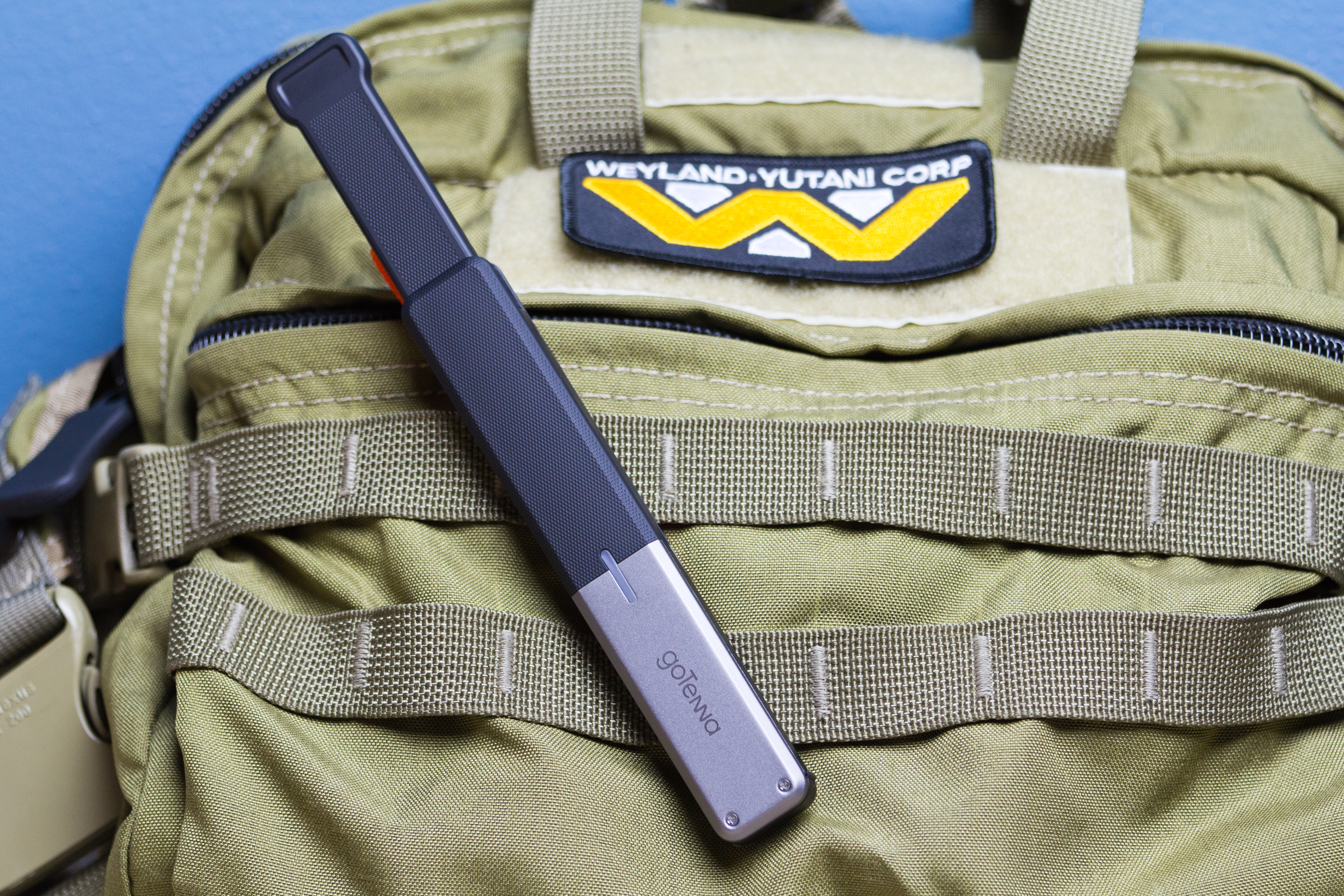
I’ve been watching the goTenna project progress with interest. At its core, it’s a commoditized radio modem available to the general public with a very low barrier to entry. It operates on the MURS band (150MHz), making it limited to operation inside the United States of America at the moment. The goTenna itself pairs with an Apple iOS or Google Android device running the goTenna app. Messages can be sent through the app to other goTenna users in the near vicinity. I’m interested in introducing computer-operated services to the network, such as physically-rooted information sources or bridges to other sources of information (like the internet). In order to do this I wanted to become familiar with the goTenna hardware and how it operates. Naturally, I did what I normally do and took it to bits.
Before I begin, I must say that I’m very impressed with the overall industrial engineering of the device itself. It feels really nice in the hand and the design seems well-thought-out. This, hopefully, speaks to the attention to detail I’ll find inside.
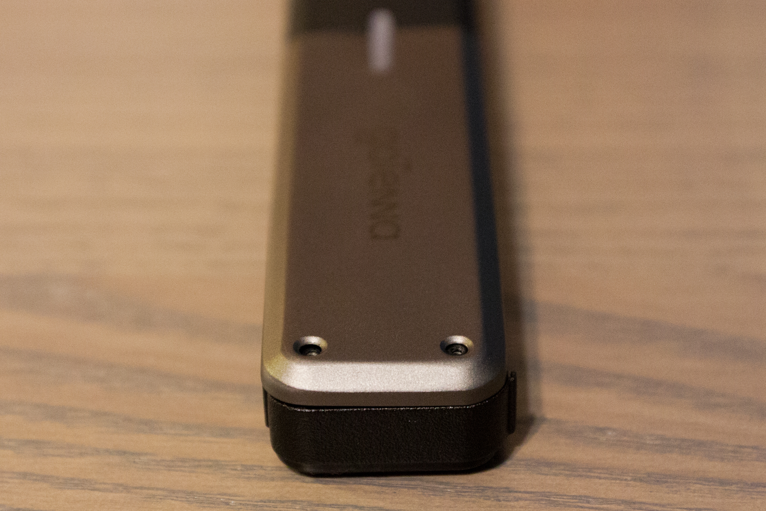
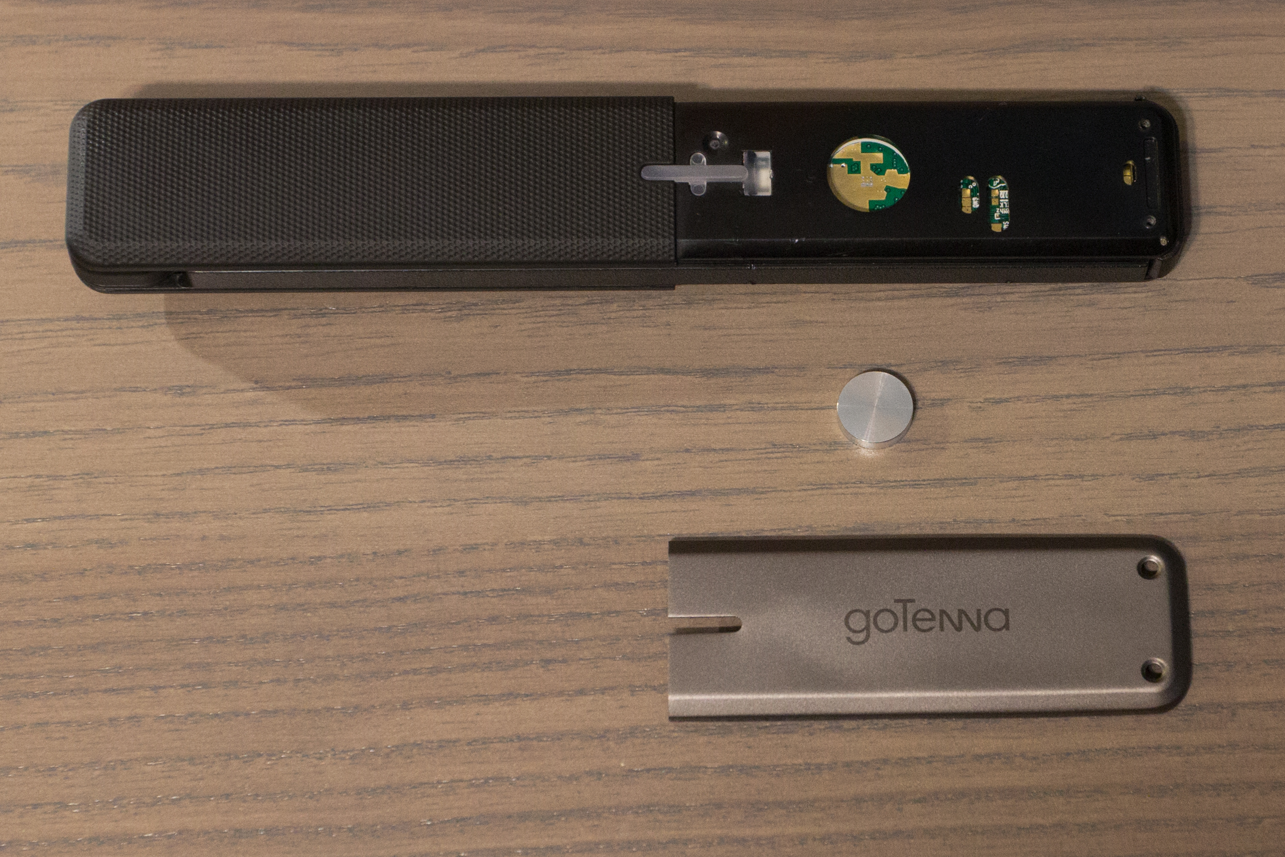
On the surface there’re few hints about how to get inside the case. The top half of the goTenna is textured plastic, and the bottom half has a metal veneer on each side. Removing the tiny screws in each metal veneer does not free them immediately. I used a metal prizing tool to lift off each veneer and discovered they’re held down by rather agressive adhesive.
Removing the top veneer reveals a few openings in the case. There are three openings for programming the device, and one larger opening in which a metal disc fits to heat sink the RF section of the PCB out to the top metal veneer. This disc was liberally covered thermal grease, which I removed prior to taking pictures.
As these openings are covered, the goTenna is likely good at keeping dust and other solid contaminants out, as advertised, but likely is not impermeable. Anyone building permanent fixtures containing a goTenna should definitely keep this in mind.
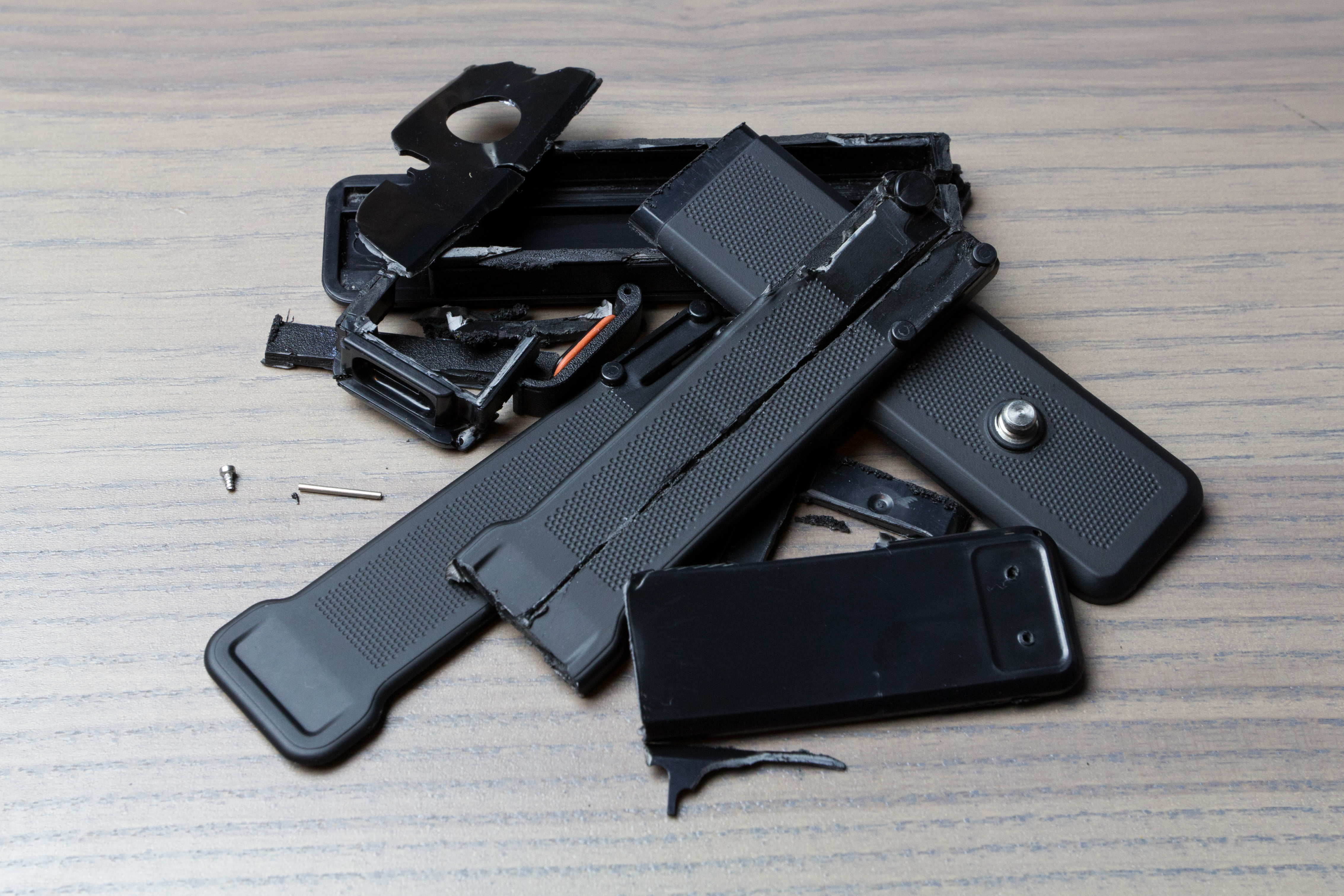
Opening the case is a horrifyingly irreversible process. Since the goTenna case is ultrasonically welded, there’s no way to get it apart other than to cut it in half. It’s critically important to be careful while doing this because there’s a lithium polymer battery nestled in, effectively, the bottom half of the device. Puncturing a lithium polymer battery results in energetic fire and toxic fumes, and therefore is best avoided at all costs.
Once inside, the PCB, attached battery, and antenna can be freed. The main radiating element of the antenna is encased in its own separate plastic shell.


Inside we find a fairly densely packed four-layer board, with most of the passives and smaller components dedicated to power management and RF. The larger and more interesting components are:
- Freescale Kinetis KL26 ARM Cortex Microcontroller MKL26Z256VMP4 (labeled as M26P8V).
- Spansion S25FL116K 16 Mbit Flash.
- Silicon Labs Si4460 Rev 1B Transceiver (marked 44601B).
- Nordic Semiconductor nRF8001 Bluetooth Smart Connectivity IC.
- Honeywell SL353LT Digital Hall Effect Sensor.
- AEC AEC601747 Lithium Polymer Battery. 350mAh at 3.7V nominal. Likely whatever battery is cheaply sourced at the time is included.
Nearly all the ICs on the PCB are low-power variants, which allows the goTenna to achieve a long run-time on such a meager battery. It does seem to get the 20 hours advertised battery life while idling.
The main ARM microcontroller is from the Freescale Kinetis family. It’s paired with the 16 Mbit flash chip from Spansion in which the programming and message buffers are kept. The goTenna is field upgradable over Bluetooth, suggesting that the flash is at least twice as large as it needs to be.
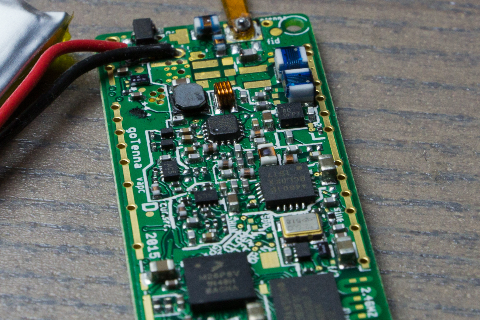
The MURS packet radio is implemented on top of the Silicon Labs Si4460 transceiver. This chip offers +13 dBm transmission power and an excellent sensitivity of -133 dBm, all while using very little current. goTenna claims 2 W of transmission power, well beyond what the chip itself can put out. I’d hazard a guess that there’s an additional amplifier stage on the PCB, but RF is beyond my knowledge.
The goTenna turns itself on and off when the antenna is extended and retracted via a Hall effect sensor located at the top of the PCB and a small magnet in the base of the antenna’s shell. This means that after the shell has been discared the goTenna is always on unless placed near a magnetic field. Additionally, the goTenna can be turned on with the antenna fully retracted by placing it near a magnetic field.
There are a few other parts of note on the PCB: one awfully bright white LED for the outside indicator light, one red LED near the USB port for charging indication, and a button near the USB port.
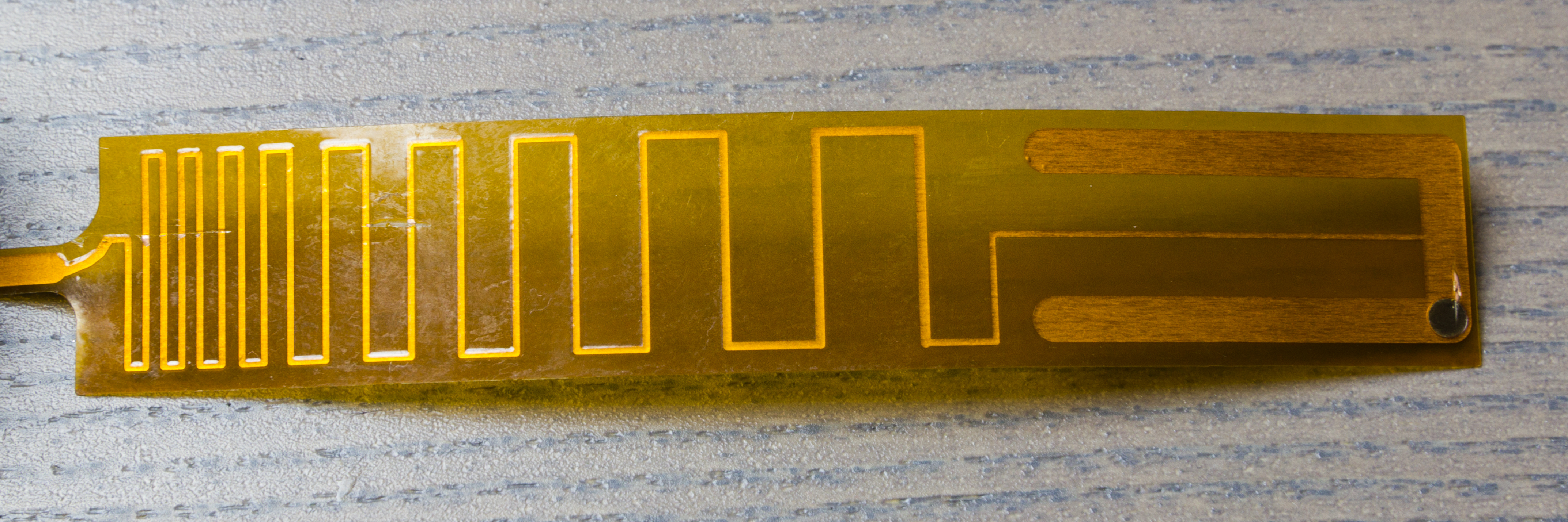
The antenna is a section of flatflex with flatflex pigtail that permits a connection as it’s extended and retracted. The final antenna seems very close to pre-production designs.
While opening the antenna’s plastic shell I accidentally cut into the antenna in a few places. While there’s good continuity across it, I’ve introduced quite a bit of attenuation. In time I plan on removing the stock antenna and soldering a SMA connector to the board.