goTenna Mesh Teardown

goTenna released their second generation wireless communication device recently, a “mesh” version appropriately named goTenna Mesh, after successfully raising funds through Kickstarter in September 2016. They started shipping in July 2017 and I received my kickstarter backed units in September 2017 in one of the last shipping batches to the US. I have been looking forward to receiving these in order to pull it apart to see what changed between the original goTenna and the new goTenna Mesh. I have previously disassembled the original goTenna.
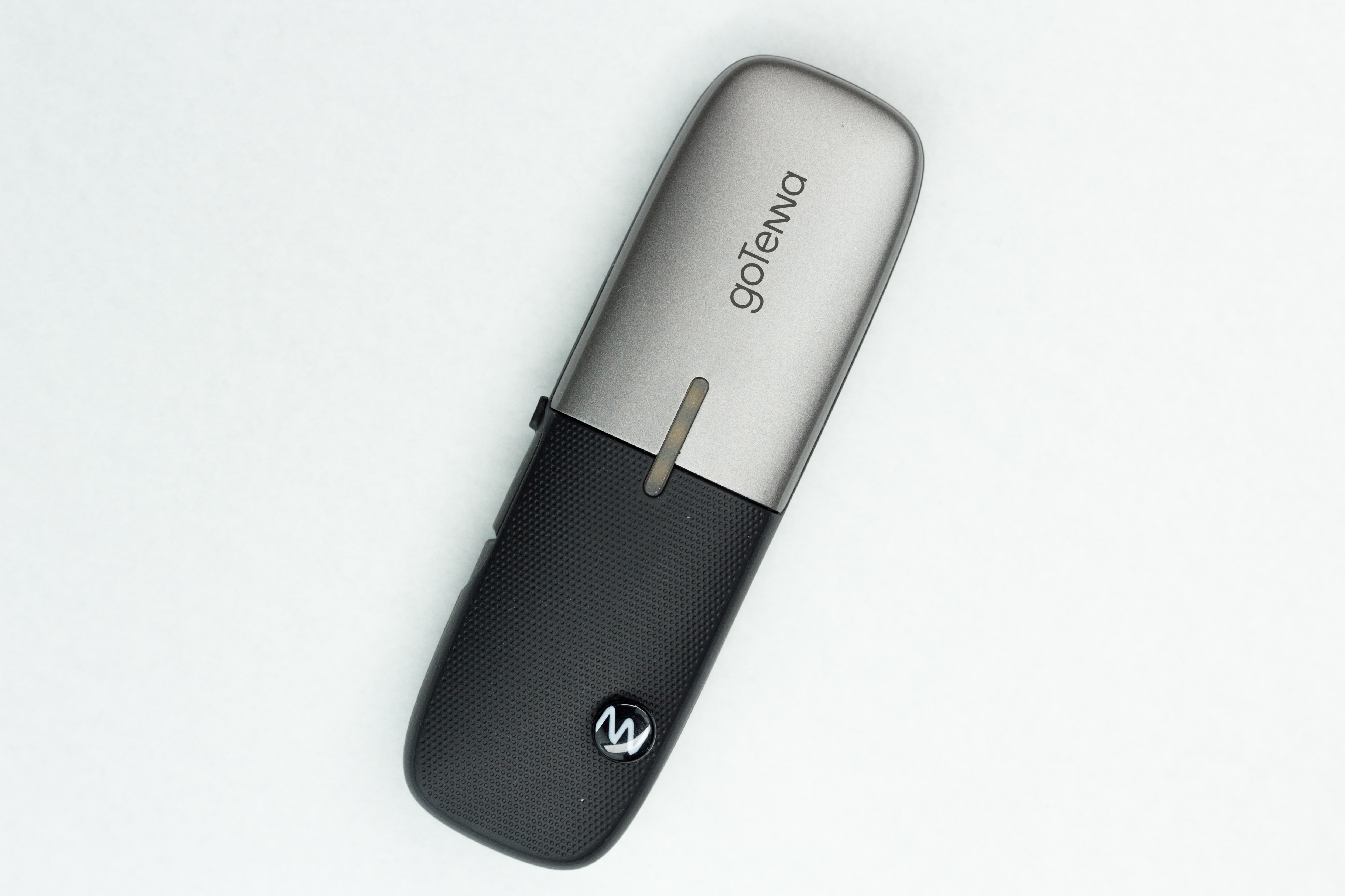
As with the original goTenna hardware released in 2015, the overall industrial design is great. The exterior pays respects to the original version, sporting a mix of dimpled ABS and brushed aluminium. The new goTenna Mesh is wider, shorter, and more curved than the original. It gives the appearance that it has been inflated internally, like a balloon. It’s a little smaller and larger in the places it needs to be, making it much more comfortable to hold in the hand.
Externally, several things changed, while others stayed the same. This could be due to more mature design for manufacturability, or cost cutting due to an increase in the bill of materials; but likely both. The attachment strap has changed from a knit fabric on the original to rubber on the goTenna Mesh, losing the expensive snaps and small screws in the process. The exterior case is of a simpler design, saving tooling expense. There’s also no longer an extendable antenna, which requied its own subassembly and hands-on time to install and solder to the main board. The removal of the extendable antenna should make the goTenna Mesh more durable.
I was aware that things likely changed internally as well. goTenna made it known that this new version operates on a new frequency (902MHz) and has new “mesh” capabilities, relaying messages through other goTenna Mesh nodes for greater reach. The change in frequency, unfortunately, means that the new goTenna Mesh is incompatible with the original goTenna. However, the move to the new frequency band (the Industrial, Scientific, and Medical (ISM) band) is exciting as it removes some of the onerous regulations that that exist on the MURS band, where the original goTenna operates. The MURS band is limited mostly to the United States and the FCC prevents connecting a MURS radio to a network (depending on whether you and the FCC can agree on what a network is). This restriction eliminates some of the more interesting things that could be done beyond simply communicating with other humans. Being unable to legally connect a goTenna to the internet prevents intelligent services or world-wide message relaying. Surprisingly, you also can’t have a MURS radio more than 60 feet above ground level.
In order to see how things changed on the inside, I needed to open it up. I started by removing the top and bottom brushed aluminum veneers to see whether there were any screws or other fasteners holding it together. These veneers are held down by adhesive tape and lift off with a bit of careful prying. They’re noticably thicker than those on the original: 0.7mm compared to 0.3mm. The increase in thickness allows them to be removed without warping or bending.

After removing the veneers I discovered that, like the original goTenna, there’s a strategically placed hole in the case over the main processor. This hole is nearly identical in size and placement to the hole on the original goTenna. On the original, a small metal disc was covered in thermal grease and placed in this hole, forming a thermal connection between the processor and top veneer. However, there’s no such disc included on the goTenna Mesh. The surface of the aluminium veneers on the goTenna Mesh are convex, which would significantly complicate a thermal connection. This could be one reason why this metal disc was ommited.
Curiously, there are no longer Serial Wire Debug (SWD) programming / diagnostic pads, or any test pads for that matter, accessible while the case is on. The main board must now be completely programmed and verified before being placed inside the case.
The top and bottom of the case are ultrasonically welded together to provide a weather-resistant seal free of screws, gaskets, or clips. I recently heard of a method to separate plastics which are joined like this by giving them firm taps around the outside with a blunt object. I used the handle of a large screwdriver and applied many very firm whacks around the edges. A little to my surprise, the two halves of the case came apart very cleanly. You’d be hard-pressed to tell the two halves were ever separated if you glued them back together.
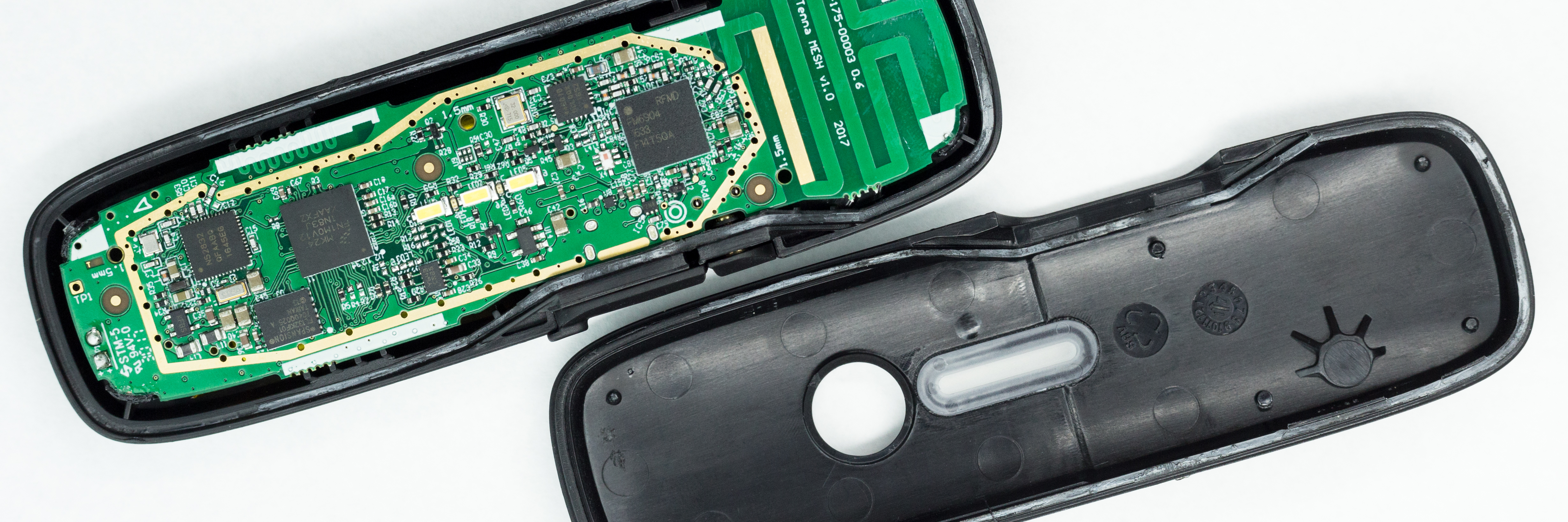
The main board and battery are held together and to the case with double-sided foam tape. The main board and battery are lifted out together fairly easily. The battery must be separated from the main board very carefully using only plastic tools. Do not bend or puncture the lithium polymer battery. Lithium-based batteries can be quite dangerous.
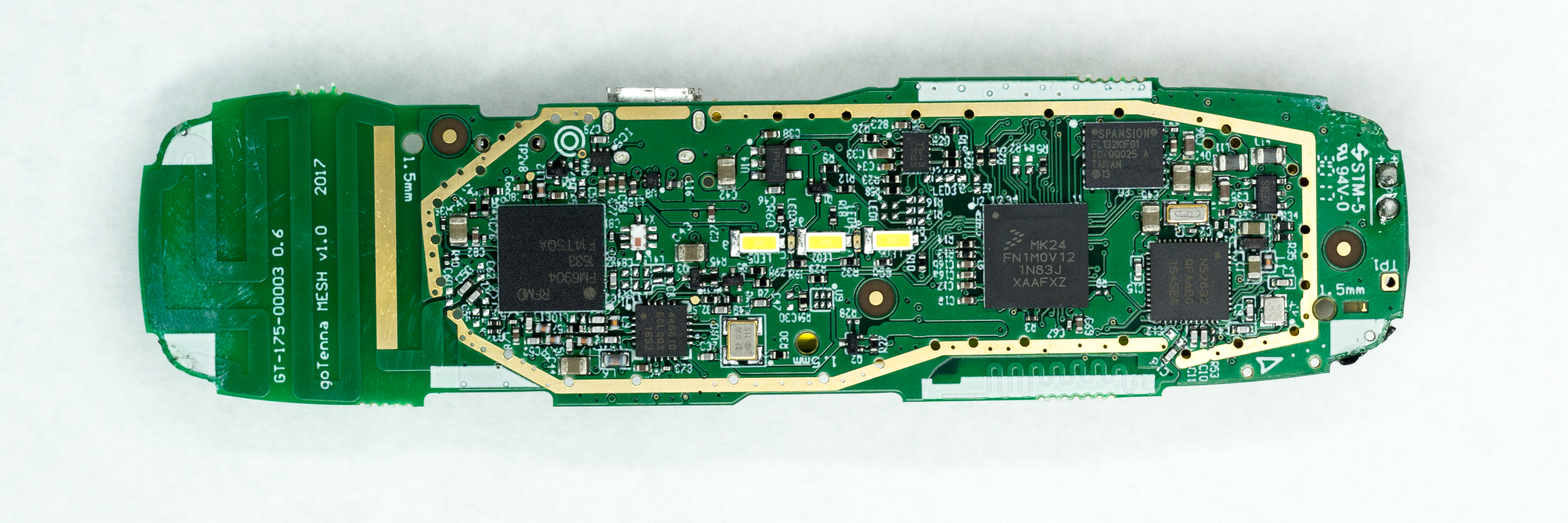
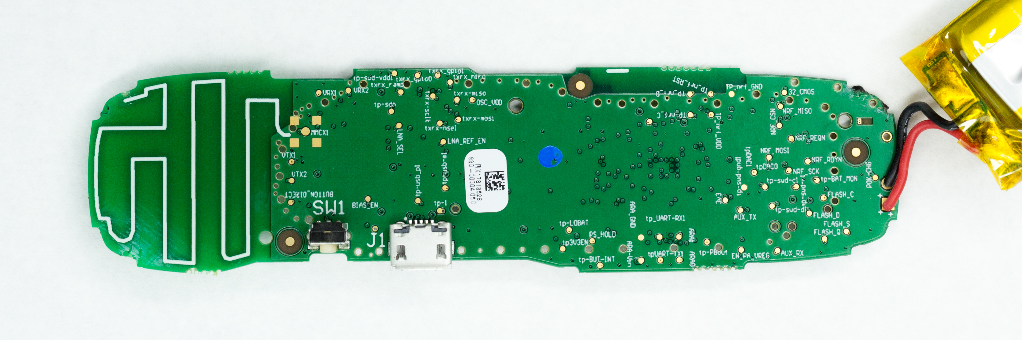
The main board is a crowded three-layer board. Nearly every component is on the top of the board, leaving the bottom for test points, a little button, and the USB port. The following are the primary and most interesting components on the board:
- Freescale Kinetis MK24 ARM Cortex Microcontroller MK24FN1M0VDC12. This is an ARM Cortex-M4 at 120MHz with 256KB of RAM.
- Spansion S25FL132KIF01 32 Mbit flash.
- Nordic Semiconductor nRF52832 Bluetooth 5 low energy / multiprotocol SoC.
- Silicon Labs Si4460 Rev 1B Transceiver (marked 44601B).
- RF Micro Devices RFFM6904 ISM Band Transmit / Receive Module.
- Three bright white surface mount LEDs.
- Two red surface mount LEDs.
- AEC AEC642147 Lithium Polymer Battery, which is 589 mAh at 3.7V nominal.
The main CPU is a 120MHz ARM Cortex-M4 from the Freescale Kinetics line of processors, which provides plenty of power. A 32 Mbit flash chip contains the firmware, message buffers, and non-volatile storage space needed for operation.
The Bluetooth transceiver, used to communicate with mobile phones running the goTenna application, is a Nordic Semiconductor nRF52832. This is a very advanced chipset supporting Bluetooth 5, Bluetooth low energy, and custom protocols in the 2.4GHz band. It also contains a complete system-on-chip ARM M4 processor. This embedded ARM M4 processor has an equivalent clock speed and CoreMark per MHz score as the main processor in the original goTenna. Having two independent ARM processors inside the goTenna Mesh may allow for interesting functionality in the future.
The packet radio is built on top of the Silicon Labs Si4460 transceiver, which is incredibly power-efficient and flexible; it operates between 119MHz and 1050MHz, covering both Region 1 and Region 2 ISM bands.
The antenna is a simple “meandering monopole” trace antenna located on the PCB, being fed by the RFFM6904. The portion of the PCB with the antenna is located under the plastic half of the exterior, not underneath the aluminum veneers.
In my previous teardown I indicated that the selection of the lithium polymer battery may have been a just-in-time manufacturing decision, allowing them to source batteries from the cheapest vendor at the time. The continued use of AEC as the battery manufacturer disproves my theory.
The evolution from the original goTenna is fairly obvious. The same vendors were used for the main CPU, flash, radio transceiver, and Bluetooth chipsets. From each vendor an identical or very similar product was selected. This is a very mature and iterative design decision, leveraging proven technologies and processes. The processor continues to be an ARM core from Freescale, but at more than double the clockspeed. The internal flash has been doubled. The transceiver chip was carried over as-is from the original goTenna, but the RF front-end has been redesigned around the RF Micro Devices RFFM6904 chip, significantly reducing the number of RF-related components on the board.
As previously noted, the goTenna Mesh operates on the 902MHz ISM band, which is applicable for all of ITU Region 2 (the Americas). The Silicon Labs Si4460 transceiver is happy to work on almost any frequency below 1GHz, but the RFFM6904 RF front-end chip is pretty specific to the Region 2 frequencies. I’m interested in how goTenna is meeting compliance obligations for units shipped to Europe and the rest of ITU Region 1, which has the ISM band down on 433MHz, well outside of where the RFFM6904 RF front-end chip can operate.
One possible way to achieve compliance is by using the RF Micro Devices RFFM6404, which is the 433MHz (Region 1) ISM version of the RFFM6904. Such a signficant change in frequency may also require a separate spin of the main board, with a different antenna.
However, on the goTenna Kickstarter FAQ, they indicate that 869MHz is used in Europe. A scant amount of Googling indicates this is a perfectly valid frequency to use, and it’s down at the bottom of the frequency range supported by the RFFM6904 RF front-end chip. It’s also near enough to 902MHz that a single antenna could work for both. Without different devices for each region, the device must somehow detect where it’s located to tune to the correct band. If this is possible, perhaps it can be also tuned to a different section of the ISM band in the US to create a fully partitioned mesh network?
I’d be interested to find out how frequency selection happens, and if the final European and international devices do, in fact, broadcast on 869MHz. As of writing, goTenna is wrapping up their regional certifications and approvals. Once they ship the international version, I’ll keep an eye out for one to crack open.